 |

Flip Chip Packaging Technology Solution
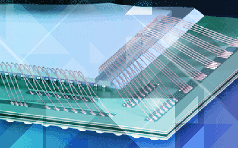
Demand for flip chip interconnect technology is being driven by a number of factors from all corners of the silicon industry. To support this demand, Amkor is committed to being the leading provider of Flip Chip in Package (FCiP) technology. By partnering with proven industry leaders, Amkor has brought high volume packaging and assembly to the subcontract market. SuperFC®, fcBGA, fcLBGA and fcCSP are qualified and are in production. Flip Chip production capability exists in our Philippines, Korea, Taiwan and China factories. Wafer Bumping, Wafer Level Packaging (WLP), and Flip Chip packaging solutions are qualified in lead-free options.
What is Flip Chip?
Flip Chip (FC) is not a specific package (like SOIC), or even a package type (like BGA). Flip Chip describes the method of electrically connecting the die to the package carrier. The package carrier, either substrate or leadframe, then provides the connection from the die to the exterior of the package. In "standard" packaging, the interconnection between the die and the carrier is made using wire. The die is attached to the carrier face up, then a wire is bonded first to the die, then looped and bonded to the carrier. Wires are typically 1-5 mm in length, and 25-35 µm in diameter. In contrast, the interconnection between the die and carrier in flip chip packaging is made through a conductive "bump" that is placed directly on the die surface. The bumped die is then "flipped over" and placed face down, with the bumps connecting to the carrier directly. A bump is typically 70-100 µm high, and 100-125 µm in diameter.
The flip chip connection is generally formed one of two ways: using solder or using conductive adhesive. By far, the most common packaging interconnect is solder Current solder types are: eutectic (63%Sn, 37%Pb) or high lead (95%Pb, 5%Sn) or lead-free (97.5%Sn, 2.5%Ag) compositions. The solder bumped die is attached to a substrate by a solder reflow process, very similar to the process used to attach BGA balls to the package exterior. After the die is soldered, underfill is added between the die and the substrate. Underfill is a specially engineered epoxy that fills the area between the die and the carrier, surrounding the solder bumps. It is designed to control the stress in the solder joints caused by the difference in thermal expansion between the silicon die and the carrier. Once cured, the underfill absorbs the stress, reducing the strain on the solder bumps, greatly increasing the life of the finished package. The chip attach and underfill steps are the basics of flip chip interconnect. Beyond this, the remainder of package construction surrounding the die can take many forms and can generally utilize existing manufacturing processes and package formats.
Benefits of Flip Chip:
Using flip chip interconnect offers a number of possible advantages to the user:
- Reduced signal inductance - because the interconnect is MUCH shorter in length (0.1 mm vs 1-5 mm), the inductance of the signal path is greatly reduced. This is a key factor in high speed communication and switching devices.
- Reduced power/ground inductance - by using flip chip interconnect, power can be brought directly into the core of the die, rather than having to be routed to the edges. This greatly decreases the noise of the core power, improving performance of the silicon.
- Higher signal density - the entire surface of the die can be used for interconnect, rather than just the edges. This is similar to the com parison between QFP and BGA packages. Because flip chip can connect over the surface of the die, it can support vastly larger numbers of interconnects on the same die size.
- Die shrink - for pad limited die (die where size is determined by the edge space required for bond pads), the size of the die can be reduced, saving silicon cost.
- Reduced package footprint - in some cases, the total package size can be reduced using flip chip. This can be achieved by either reducing the die to package edge requirements, since you no longer have to leave space for wires, or in utilizing higher density sub strate technology, which allows for reduced package pitch.
Wafer Bumping Technology:
Amkor offers state-of-the-art wafer bumping capability in electroplated solder technologies in multiple strategic locations (Taiwan, Korea, Singapore, and the US). These locations are uniquely situated adjacent to major foundry sources to enable our customers reduced time to market with integrated factory logistics. Amkor’s bumping is based on its proprietary electroplating solder technology which is considered the most advanced, robust, reliable and high yielding process available in the marketplace. Low Alpha Eutectic, High Lead, and Lead-free are in high volume production at all facilities. 300 mm wafer bumping production is offered in the Taiwan facility.
Features:
- Wafer sizes from 150 mm to 300 mm diameter
- Full area array pitch available to 175 µm -- perimeter pad pitch to 125 µm
- Solder compositions ranging from 63Sn/37Pb, 95Pb/5Sn, 97.5Sn/2.5Ag (all available as low alpha: <0.02 cts/hr/cm2), SnAgCu
- Redistribution and repassivation using either BCB or polyimide
- Multi-Level Thin Film structure and Interconnect Passives with Solder Bump
- Wafer Level Packaging (WLP)
- Worldwide design support
Packaging Options Using Flip Chip:
Depending on the specific die and application requirements, different package level solutions are required. Thus flip chip interconnect can be used in a wide range of package solutions, each focused on specific benefits that serve a given market. Amkor offers the widest possible range of flip chip packaging solutions to meet the diverse needs of customers and end users. Combining their extensive manufacturing knowledge with all types of packaging interposers and further leveraging their leadership role in flip chip interconnect technology, Amkor continues to pursue new package solutions. This kind of focus is essential to insure that as new market needs emerge requiring flip chip interconnect, Amkor is ready with the optimum package to meet those needs.
fcCeramic CBGA / CLGA / CLLGA / Solder Column Interposer:
Flip chip packaging solution for most of flip chip's history.
Features:
- 5-20 layers, Alumina and HiTCE
- Target Market - Internet Workstation Processors, High Bandwidth System Communications Devices, Printer Applications
- Lidded and unlidded versions, LGA and BGA, Solder Column Interposer, Passive Attach
- 200 µm minimum bump pitch
- Die sizes up to 21 mm
- Package sizes from 27 mm to 50 mm
- 0.8, 1.0 mm and 1.27 mm pitch footprint
- Bare die or AISiC lid
fcBGA / fcLGA (Bare Die):
Flip chip packaging solution for most graphics, PC chipset, and low end ASIC applications.
Features:
- 4-8 layer build up substrates using epoxy laminate
- Bare die, Passive attach
- 200 µm minimum bump pitch for laminate
- Die sizes up to 16.7 mm
- Package sizes from 27 mm to 37.5 mm
- JEDEC MS-034 compliant, 1.0 mm pitch BGA footprint
- Stacked vias
- MRT
- Stiffener option for large die
- Motherboard TCE match (HITCE)
- Low Warpage
- Solid ground planes
- Close substrate to silicon TCE match reduces stress on die surface
- Thermal dissipation (AI203)
- Current mainstream Flip Chip package for chipset and graphics applications
- Lowest cost construction
SuperFC® Package:
Amkor Technology is now offering SuperFC® packaging, the super performance flip chip solution. Flip chip interconnect utilizes array interconnect of die to substrate as a replacement for conventional wire bonding. This allows the entire die surface to be used for electrical connections to the substrate, exponentially increasing the I/O per unit area vs. perimeter interconnect technologies. Implementing process technology licensed from industry leader LSI Logic, Amkor’s SuperFC® package uses solder bump flip chip interconnect, and can route over 1000 signal traces from a single die out to a 1.0 mm pitch BGA footprint.
SuperFC® packages are assembled around state-of-the-art laminate substrates. Utilizing multi-layer, blind and buried vias, laser drilled build-up structures, and ultra fine line/space metallization, SuperFC® has the highest routing density BGA available. Using flip chip interconnect automatically improves package electrical performance by removing the high inductance wires and replacing them with low inductance solder connections. By combining flip chip with ultra advanced substrate technology, packages can be electrically tuned for maximum electrical performance.
Features:
- 4-10 layer build up substrates using epoxy laminate
- Target Market - Internet Workstation Processors, High Bandwidth System Communications Devices
- Veriety of heatspreader options, passive attach
- 175 µm minimum bump pitch
- Die sizes up to 16.7 mm, extending to 21 mm
- Package sizes from 27 mm to 50 mm, passive attach
- JEDEC MS-034 compliant, 1.0 mm pitch BGA footprint
- Package solutions up to 2400 balls
fcCSP Package:
Flip Chip solution for CSP package technology.
Features:
- Designed for high frequency applications Target Market - Cell Phones, Hand-held Electronics Thin core laminate or ceramic package construction
- Overmolded for handling and second level reliability
- Accommodates package sizes from 3 mm to 15 mm
- Combine with passives in RF PA module applications
- Flip Chip bump pitches of 150 µm min. for peripheral array, 250 µm min. for area array
- Available in 0.5 mm - 1.0 mm BGA ball pitch, as well as LGA interconnect
- Primary drivers are elctrical performance and form factor
- Minimum package thickness of 0.80 mm for LGA interconnect, 1.0 mm for 0.5 mm BGA pitch and 1.2 mm for 0.8 mm BGA pitch
- Flip Chip version of Amkor ChipArray®
- Array strip production, overmold and singulate
Flip Chip SiP Package:
Flip Chip SiP package is an extension of the SiP product offering from Amkor with the device interconnect technology being flip chip rather than traditional wirebond interconnects. The package may contain multiple passive components, Silicon and/or GaAs devices bumped with traditional solder bumps or solder coated 'Copper-Pillar' bumps housed in 2-Layer or 4-Layer high density substrates. This package format is gaining traction in RF Power Amplifier and RF Front End module applications for size, performance and cost reasons. Controlled collapse of the bumps leads to predictable interconnect impedance and hence more stable product performance. The low solder volume in the 'wetting tip' allows for the elimination of the soldermask from underneath the die which reduces the substrate complexity and cost and removes a major barrier for adopting the fine pitch FC interconnection technology in the RF application space. Flip chip interconnection may also preclude the need for wafer backgrinding (for mold cap thickness ≥ 0.9 mm) which leads to further reduction in product cost and simplification of the process flow.
The devices in this application space have low to medium I/O count and are fairly small in size. This, in conjunction with the solder mask being removed from underneath the die (which increases the standoff), makes these products viable candidates for transfer molding applications. Thus, the underfill operation can be eliminated from the process flow, which leads to significant cost savings. Studies have shown that transfer molded packages are more reliable (MSL as well as extended reliability testing such as Temperature cycling, HAST, etc.) than their underfilled counterparts due to balanced die stresses and better solder CTE matching.
Wafer Level Packaging: CSPnl™:
CSPnl™ is a true wafer level package to address improved second level board reliability, that incorporates is designed to utilize standard surface mount assembly and reflow techniques. By using standard SMT placement equipment, and avoiding the need for underfill, the end user experiences many of the cost benefits associated with other JEDEC standard area array packages.
Features:
- Incorporates standard JEDEC pitches and CSP solder ball diameters
- Compatible with standard SMT assembly and test techniques
- Utilizes cost-effective thin film redistribution technologies
- Backside laser mark compatible
- Impressive component and board level reliability
- No need for underfill in most applications
- Full turnkey CSPnl™ processing including test, and tape and reel support
- Eutectic high lead and lead-free solder balls
- Available with either BCB or polyimide repassivation
- Qualified and in volume production
- Proven reliability; exceeds all current handset mechanical reliability tests including: drop, bend and key punch
Additional Information:
| Description |
File Type |
File Size |
| Flip Chip Packaging Technology Solution Sheet |
 |
318 kb |
Flip Chip Packaging Technology Solution Sheet
(Japanese Translation) |
 |
1.0 MB |
| fcCSP Data Sheet |
|
120 kb
|
| SuperFC® Data Sheet |
|
132 kb
|
| CSPnl™ Wafer Level Packaging Data Sheet |
|
161 kb
|
| FlipChips Dot Com - An information resource for flip chip microelectronics. |
|
|
For more information on Flip Chip Packaging please contact an Amkor Regional Sales Office near you, contact your Account Manager or fill out a Request for Additional Information. |
 |