
An unrivaled global footprint
Corporate Headquarters
Factories
Customer Support Centers
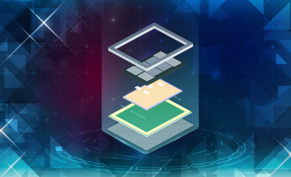
Looking for technical information?

Data Sheets

Brochures

White Papers

Articles
Want to work at Amkor?
Amkor has great career opportunities around the world. Want to learn more? Choose your region below and take the next step to joining our team.
Latest Blog Posts
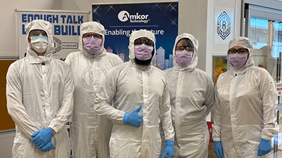
Amkor Technology Launches Semiconductor Educator Bootcamp to Strengthen Future Workforce Pipeline
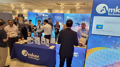
Amkor Showcases Next-Gen Packaging and U.S. Expansion at ECTC 2026
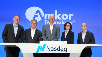
Amkor Technology Concludes 2026 Investor Day with Nasdaq Closing Bell Ceremony
Upcoming Events

TSMC 2026 China Technology Symposium Ecosystem Pavilion